Instruction Cycle
A program residing in the memory unit of the computer consists of a sequence of instructions. The program is executed by the computer through a cycle for each instruction. Each instruction cycle is subdivided into a sequence of subcycles or phases. In the basic computer, each instruction cycle consists of the following phases:
- Fetch an instruction from memory.
- Decode the instruction.
- Read . Upon the completion of step 4, the control returns to step 1 to fetch, decode, and execute the next instruction. This process continues indefinitely unless a HALT instruction is encountered.

Fetch and Decode
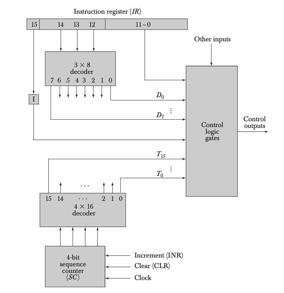
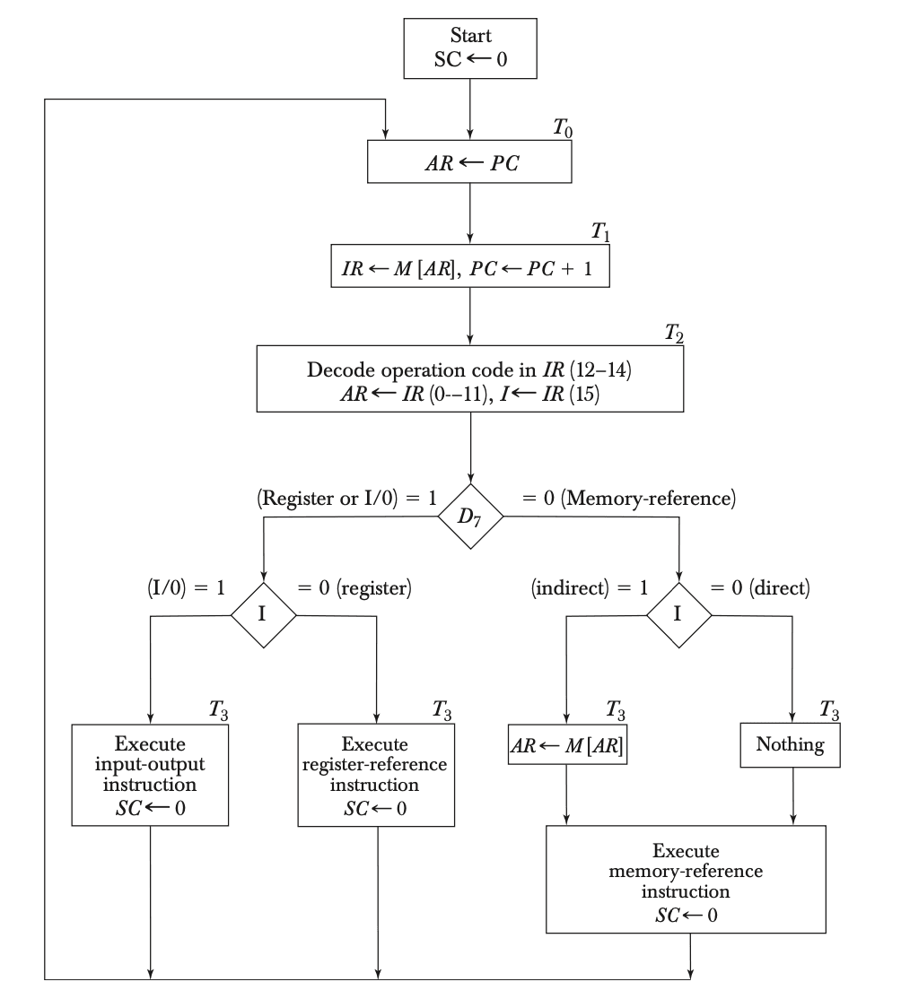
Initially, the program counter (PC) is loaded with the address of the first instruction in the program. The sequence counter (SC) is cleared to 0, providing a decoded timing signal . After each clock pulse, SC is incremented by one, so that the timing signals go through a sequence , , , and so on. The micro-operations for the fetch and decode phases can be specified by the following register transfer statements:
Since only the address register (AR) is connected to the address inputs of memory, it is necessary to transfer the address from PC to AR during the clock transition associated with timing signal . The instruction read from memory is then placed in the instruction register (IR) with the clock transition associated with timing signal . At the same time, PC is incremented by one to prepare it for the address of the next instruction in the program. At time , the operation code in IR is decoded, the indirect bit is transferred to flip-flop I, and the address part of the instruction is transferred to AR. Note that SC is incremented after each clock pulse to produce the sequence , , and .
To provide the data path for the transfer of PC to AR, we must apply timing signal to achieve the following connection:
- Place the content of PC onto the bus by making the bus selection inputs equal to 010.
- Transfer the content of the bus to AR by enabling the LD input of AR.
The next clock transition initiates the transfer from PC to AR since . In timing signal , it is necessary to use the following connections in the bus system:
- Enable the read input of memory.
- Place the content of memory onto the bus by making .
- Transfer the content of the bus to IR by enabling the LD input of IR.
- Increment PC by enabling the INR input of PC.
The next clock transition initiates the read and increment operations since .
Determine the Type of Instruction
The timing signal that is active after the decoding is . During time , the control unit determines the type of instruction that was just read from memory. The three possible instruction types available in the basic computer are:
- Memory-reference instruction
- Register-reference instruction
- Input-output instruction
The decoder output is equal to 1 if the operation code is equal to binary 111. If , the instruction is either a register-reference or input-output type. If , the operation code specifies a memory-reference instruction. Control then inspects the value of the first bit of the instruction, which is now available in flip-flop I. If and , the instruction is a memory-reference instruction with an indirect address. It is then necessary to read the effective address from memory. The micro-operation for the indirect address condition can be symbolized by the register transfer statement:
Initially, AR holds the address part of the instruction. This address is used during the memory read operation. The word at the address given by AR is read from memory and placed on the common bus. The LD input of AR is then enabled to receive the indirect address that resided in the 12 least significant bits of the memory word.
The three instruction types are subdivided into four separate paths. The selected operation is activated with the clock transition associated with timing signal . This can be symbolized as follows:
: Execute a register-reference instruction
: Execute an input-output instruction
:
When a memory-reference instruction with is encountered, it is not necessary to do anything since the effective address is already in AR. However, the sequence counter SC must be incremented when , so that the execution of the memory-reference instruction can be continued with timing variable . A register-reference or input-output instruction can be executed with the clock associated with timing signal . After the instruction is executed, SC is cleared to 0, and control returns to the fetch phase with .
Note that the sequence counter SC is either incremented or cleared to 0 with every positive clock transition. We adopt the convention that if SC is incremented, we will not write the statement , but it will be implied that the control goes to the next timing signal in sequence. When SC is to be cleared, we will include the statement .
Register-Reference Instructions
Register-reference instructions are recognized by the control when and . These instructions use bits 0 through 11 of the instruction code to specify one of 12 instructions. These 12 bits are available in . They were also transferred to AR during time .
The control functions and micro-operations for the register-reference instructions are listed below. These instructions are executed with the clock transition associated with timing variable . Each control function needs the Boolean relation , which we designate for convenience by the symbol . The control function is distinguished by one of the bits in . By assigning the symbol to bit of IR, all control functions can be simply denoted by . For example, the instruction CLA has the hexadecimal code 7800, which gives the binary equivalent 0111 1000 0000 0000. The first bit is a zero and is equivalent to . The next three bits constitute the operation code and are recognized from decoder output . Bit 11 in IR is 1 and is recognized from . The control function that initiates the micro-operation for this instruction is . The execution of a register-reference instruction is completed at time . The sequence counter SC is cleared to 0, and the control goes back to fetch the next instruction with timing signal .
The first seven register-reference instructions perform clear, complement, circular shift, and increment micro-operations on the AC or E registers. The next four instructions cause a skip of the next instruction in sequence when a stated condition is satisfied. The skipping of the instruction is achieved by incrementing PC once again (in addition to it being incremented during the fetch phase at time ). The condition control statements must be recognized as part of the control conditions. The AC is positive when the sign bit in ; it is negative when . The content of AC is zero () if all the flip-flops of the register are zero. The HLT instruction clears a start-stop flip-flop S and stops the sequence counter from counting. To restore the operation of the computer, the start-stop flip-flop must be set manually.
